|
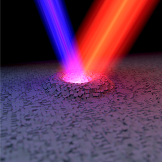
All-dielectric Plasmonics Dr. M. Ferrera is among the initiators of the new field of all-dielectric plasmonics which make use of novel Transparent Conducting Oxides (TCOs) to solve all the fundamental technological issues plaguing today’s plasmonic components such as high losses, lack of tunability, and incompatibility with standard semiconductor fabrication processes. TCOs enables the epsilon-near-zero (ENZ) regime at fundamental telecom wavelengths and without the use of structured materials. The ENZ behaviour of TCOs together with their giant complex nonlinearities allows the ultimate level of control in engineering photon emission |
SiN photonics
The Advanced Structured Nanophotonics Lab has traditionally been oriented towards the realization of integrated nonlinear photonic devices based on silicon nitride (SiN). This material, which has been routinely used by the semiconductor industry since 1990 for the fabrication of CMOS components, has recently entered the world of photonics demonstrating great potential. Silicon nitride is not affected by two-photon and free carrier absorption and possess a nonlinear Kerr coefficient which is 10 times larger than that for silica glass. Its fabrication process are well developed and ultra-low loss (<0.1dB/cm) waveguides and high quality factor resonators have already been demonstrated. For all these reason, SiN is the perfect candidate for future all-optical integrated circuitry, and our lab wants to continue producing valuable results in this direction.
Quantum optics
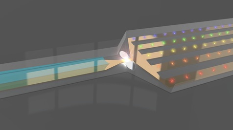
Dr. Marcello Ferrera has a long experience in the design, fabrication, and characterization of integrated photonic devices for efficient on-chip nonlinear frequency conversion. These nonlinear elements could constitute the backbone of very fundamental quantum systems such as single- and entangled-photon sources. One of the goals of the ASN Lab is to exploit this know-how to merge Nanophotonics and nonlinear optics in order to obtain the first fully integrated quantum plasmonic module. In order to achieve this ambitious goal, diamond and in general carbon-based optical systems, are also taken in consideration.
Dr. Marcello Ferrera has a long experience in the design, fabrication, and characterization of integrated photonic devices for efficient on-chip nonlinear frequency conversion. These nonlinear elements could constitute the backbone of very fundamental quantum systems such as single- and entangled-photon sources. One of the goals of the ASN Lab is to exploit this know-how to merge Nanophotonics and nonlinear optics in order to obtain the first fully integrated quantum plasmonic module. In order to achieve this ambitious goal, diamond and in general carbon-based optical systems, are also taken in consideration.

Flexible photonics
Most electronic and opto-electronic components are based on a planar technology built on top of a rigid semiconductor substrate. This is necessary to ensure that all the constituent materials possess the required electrical, mechanical and optical properties for the targeted functionality. However, modern society asks for an even deeper penetration of science and technology into all aspects of our life, and this request needs more versatile and “flexible” basic materials. For these reasons, numerous research activities are currently ongoing in many nanophotonic labs all over the world with the final goal of designing, fabricating, and testing prototypes of flexible photonic devices in order to determine how the properties of these components are affected by deformation and mechanical strain.
Most electronic and opto-electronic components are based on a planar technology built on top of a rigid semiconductor substrate. This is necessary to ensure that all the constituent materials possess the required electrical, mechanical and optical properties for the targeted functionality. However, modern society asks for an even deeper penetration of science and technology into all aspects of our life, and this request needs more versatile and “flexible” basic materials. For these reasons, numerous research activities are currently ongoing in many nanophotonic labs all over the world with the final goal of designing, fabricating, and testing prototypes of flexible photonic devices in order to determine how the properties of these components are affected by deformation and mechanical strain.
DNA-based nanophotonics
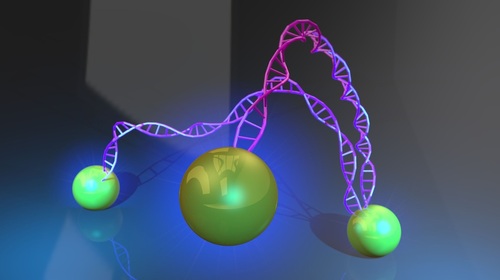
A very new branch of Nanophotonics, which can certainly revolutionize the way we think and live, is the so-called DNA photonics. Scientists have started looking at DNA not only from the biological point of view but also as a formidable programmable building block for the fabrication of nanostructures. On the one hand, the possibility of linking DNA strings to metallic nano-particles in a specific crystallographic framework could allow one to tailor the electromagnetic response following a bottom-up strategy. On the other hand, by arranging the DNA sequence at will and exploiting the intrinsic reproduction properties of the molecule of life, we could have access to nearly unlimited, ultra-low-cost data storage and copying. The ASN Lab believes that the next technological epoch will happen at the intersection of photonics, biology, and chemistry.
A very new branch of Nanophotonics, which can certainly revolutionize the way we think and live, is the so-called DNA photonics. Scientists have started looking at DNA not only from the biological point of view but also as a formidable programmable building block for the fabrication of nanostructures. On the one hand, the possibility of linking DNA strings to metallic nano-particles in a specific crystallographic framework could allow one to tailor the electromagnetic response following a bottom-up strategy. On the other hand, by arranging the DNA sequence at will and exploiting the intrinsic reproduction properties of the molecule of life, we could have access to nearly unlimited, ultra-low-cost data storage and copying. The ASN Lab believes that the next technological epoch will happen at the intersection of photonics, biology, and chemistry.
